A p-type silicon wafer is a foundational material in the semiconductor and photovoltaic industries, and its quality directly determines the performance of final electronic devices. Manufacturing a high-quality p-type wafer involves a series of highly controlled processes, starting from raw silicon purification to crystal growth, doping, slicing, polishing, and final inspection. Each stage must meet strict industrial standards to ensure purity, uniform electrical properties, and structural stability. Because even microscopic defects can affect chip performance, the production of a p-type silicon wafer requires advanced equipment, precision engineering, and rigorous quality control throughout the entire manufacturing chain.
Raw Material Purification and Silicon Refinement
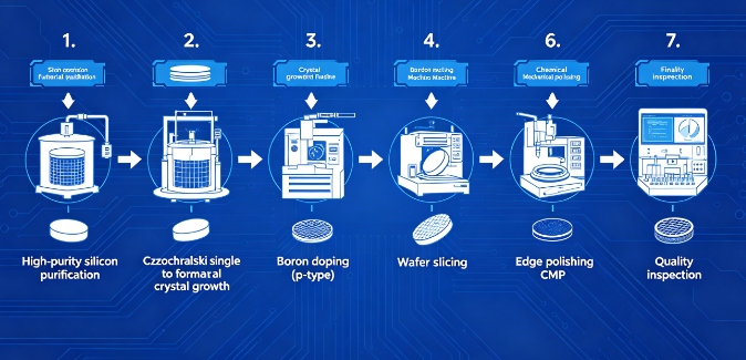
The first step in producing a high-quality p-type silicon wafer is obtaining ultra-pure silicon materials.
- Quartz extraction and reduction process: High-purity quartz is refined in high-temperature furnaces to produce metallurgical-grade silicon.
- Chemical purification stage: The silicon is further processed into chemical-grade purity using methods such as the Siemens process, reducing impurities to extremely low levels.
- Impurity control importance: Elements like oxygen, carbon, and metal contaminants must be minimized to ensure electrical stability.
- Preparation for semiconductor grade: The purified silicon is converted into electronic-grade silicon, which serves as the base material for wafer production.
This stage ensures that the foundation of the wafer meets strict semiconductor purity requirements.
Single Crystal Growth and Ingot Formation
Once purified, silicon is ready; it is transformed into a single crystal structure, which is essential for wafer consistency.
- Czochralski (CZ) method: A seed crystal is dipped into molten silicon and slowly pulled upward to form a cylindrical single crystal ingot.
- Temperature control precision: The melting and pulling process must be carefully controlled to avoid crystal defects and dislocations.
- Uniform crystal structure formation: A consistent lattice structure ensures stable electrical behavior across the entire wafer.
- Ingot shaping process: The cylindrical crystal is cooled and trimmed into a uniform ingot suitable for slicing.
This step is critical in determining the structural integrity of the final p-type silicon wafer.
Boron Doping Process for P-Type Characteristics
The defining step in creating a p-type silicon wafer is the introduction of boron doping to achieve the desired electrical properties.
- Boron incorporation during growth: Boron atoms are added into the molten silicon during crystal formation to create positive charge carriers (holes).
- Controlled doping concentration: Precise regulation of boron levels ensures consistent resistivity across the wafer.
- Uniform electrical property distribution: Proper mixing techniques prevent uneven doping, which could lead to performance instability.
- Quality monitoring systems: Real-time measurement tools are used to track dopant distribution during crystal growth.
This doping process is what distinguishes p-type wafers from other semiconductor materials.
Wafer Slicing, Shaping, and Surface Processing
After crystal growth, the silicon ingot is processed into thin wafers suitable for semiconductor fabrication.
- Precision slicing using wire saws: The ingot is cut into ultra-thin slices with minimal material loss and surface damage.
- Edge rounding and shaping: Wafer edges are polished to reduce cracking risks during handling and manufacturing.
- Lapping and flattening process: Mechanical and chemical processes are used to ensure uniform thickness and surface flatness.
- Surface cleaning and defect removal: Specialized chemical treatments remove microscopic particles and damage layers.
These steps ensure that each p-type silicon wafer has a smooth and stable physical structure.
Polishing, Cleaning, and Quality Inspection
Surface quality and defect control are essential for ensuring semiconductor-grade wafers.
- Chemical mechanical polishing (CMP): This process creates an ultra-smooth mirror-like surface essential for chip fabrication.
- Advanced cleaning procedures: Ultra-pure water and chemical solutions remove remaining contaminants.
- Electrical performance testing: Resistivity, carrier concentration, and uniformity are carefully measured.
- Defect detection systems: Optical and laser inspection tools identify micro-cracks, particles, and surface irregularities.
Only wafers that pass strict inspection standards are classified as high-quality p-type silicon wafers.
Conclusion
The manufacturing of a high-quality p-type silicon wafer involves multiple precise and highly controlled stages, including silicon purification, crystal growth, boron doping, wafer slicing, surface polishing, and final inspection. Each step plays a vital role in ensuring structural integrity, electrical stability, and surface perfection. Through advanced technology and strict quality control, manufacturers can produce wafers that meet the demanding requirements of the semiconductor and photovoltaic industries. As a result, p-type silicon wafers remain a critical material supporting modern electronics and renewable energy technologies worldwide.
0